Accessing IoT Device Secrets
Dumping Data from an SPI Flash Memory
Modern IoT device manufacturers produce a wide-range of devices that often share similar software or secrets such as API or TLS keys (e.g., a Smart Plug and a Smart Bulb). An attacker who gains access to one device can replicate the same attack on the other. Because embedded device (IoT) firmware architects tend to prioritize functionality over security, exploiting SPI flash and other device components is becoming common.
IoT devices offer a lot of functionality and provide users multiple ways to interact with them (e.g. Bluetooth, WiFi, mobile applications, etc). In order to support all these functions, they require firmware.
Firmware allows developers to have low-level control of the device and hardware and also can be used to store assembly instructions, code, API keys, TLS certificates, and support files required for the effective functioning of the IoT device.
IoT devices usually have a small form factor, so energy efficient storage is required for storing the firmware. Serial flash is a small, low-power flash memory that can be used for storing firmware in IoT devices. Serial flash requires few wires on the board, thereby reducing the board space, power consumption, and overall cost.
Serial Peripheral Interface (SPI) is an industry standard protocol for providing access to the data on the serial flash. While Serial Flash is an energy efficient way to store the firmware in IoT devices, an attacker can also access data stored in the serial flash to gain access to hard-coded secrets such as API Keys, encryption keys, TLS Certificates, etc.
The Serial Peripheral Interface (SPI) is an interface bus that provides full duplex,
synchronous serial communications between microcontrollers and peripherals. Full duplex
mode means the sender and receiver can transmit and receive data at the same time. This
data is transmitted one bit at a time sequentially over a communication channel. SPI devices
use a master-slave architecture with a single master and multiple slaves. They also use a
Slave Select (SS) signal to select which slave to send data when multiple slaves are
connected to a master. It is also known as 4-Wire Serial Interface (figure below).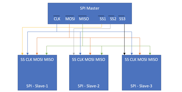
SPI specifies four logic signals, explained as follows:
Master Output and Slave In (MOSI): This pin is used to transmit data out of the SPI
module when it is configured as a Master, and receive data when it is configured as
Slave.
Master In and Slave Out (MISO): This pin is used to transmit data out of the SPI
module when it is configured as a Slave, and receive data when it is configured as
Master.
Slave Select (SS): This pin is used to output the select signal from the SPI module to
another peripheral with which a data transfer is to take place when its configured as
a Master, and its used as an input to receive the slave select signal when the SPI is
configured as Slave.
Serial Clock (SCK): This pin is used to for the clock signal. The clock signal is used to
determine the speed of data transfer.
SPI Interface and IoT Devices
Manufacturers offer a wide range of SPI Flash Memory products which are designed to
provide an effective way to store the boot code for the device with high reliability and
performance levels. The SPI Flash Memory supports the SPI interface. The majority of IoT
devices, embedded devices, and smartphones utilize the SPI Flash Memory for storing boot
code and firmware.
Attack in Action
In this section, we will explore the internals of a home router TP-LINK WR841N, identify the
SPI Flash chip, and verify if we can retrieve sensitive data from the SPI flash.
We will use the following hardware and software setup:
Hardware:- TP-LINK WR841N
- SOIC8 SOP8 Flash Chip IC Test Clips Socket
- Attify Badge (2.0)
- Tools to open the IoT device
Software:
1. EXPLORING THE DEVICE (TP LINK WR841N):
When you open the TP LINK WR841N router and gain access to the internals, you can
see that there are a few embedded chips and other hardware components.
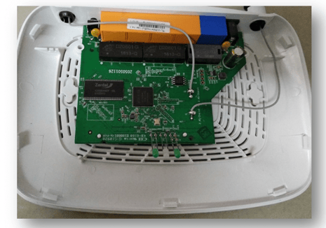
2. IDENTIFYING THE INTERNALS:
There are 3 embedded chips on the board that stand out, and each of them are labelled
with part numbers and manufacturer names.
i. Zentel A3S56D40GTP
ii. Mediatek - MT7628NN
iii. GD 25Q32CSIG
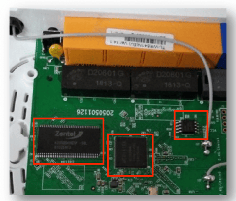
3. Exploring the Devices and Identifying Functionality:
Download the datasheets for the identified chips, and explore the features they support. Our objective is to identify the SPI Flash Memory.
• Zentel A3S56D40GTP - is a DDR SDRAM
• Mediatek - I2C, I2S, SPI, PCM, UART, JTAP, GPIO. It supports the SPI interface
• GD 25Q32C - 32M-Bit Serial Flash. Supports Dual, QUAD SPI
4. Choosing the Target Embedded Device for further Exploration:
At this point, we have identified that 2 of the ICs we observed support SPI interface. Let's pick the Serial Flash GD 25Q32C as our target for further exploration. GD 25Q32C is a serial flash, which potentially will contain the device’s firmware.
5. EXPLORING THE GD 25Q32C SPI INTERFACE:
As we saw earlier the SPI specifies four signals MOSI, MISO, Slave Select and Serial Clock. Let’s explore the GD 25Q32C data sheet to identify the SPI signals.
 .
.
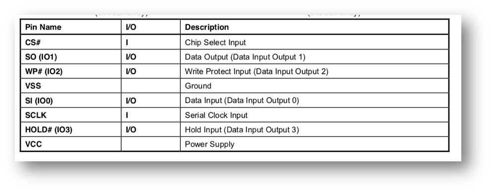
6. Connecting the Pins to the SOIC 8:
Once we have identified the SPI interface, we have to connect to it another SPI interface and try to read or write data to GD 25Q32C SPI Flash memory.
We will use the Attify Badge 2.0 as our SPI interface to interact with the GD 25Q32C SPI Flash memory. There are two ways to connect the Attify Badge to the GD 25Q32C SPI Flash memory.
- We can de-solder the IC from the PCB and proceed with the connection.
- We can use a SOIC8 IC Test Clips Socket.
We will use the SOIC8 IC Test Clips Socket. Using it helps to avoid the messy and tricky unsoldering of the chip. It can be used to directly interact with the SPI Flash memory when it is on the PCB.
7. Connecting the Attify Badge to GD 25Q32C Flash chip:
Connections between the Attify badge and the GD 25Q32C SPI Flash chip are listed below:
|
Attify Badge |
GD 25Q32C |
|
D0 |
SCLK |
|
D1 |
SO (IO1) |
|
D2 |
SI (IO0) |
|
D3 |
CS# |
|
3.3v |
WP# |
|
3.3v |
HOLD# |
|
GND |
GND |
|
3.3v |
VCC |
After setup, connect the Attify badge to a laptop. We need not provide any external power supply to the SPI flash chip, in order to read or write data.
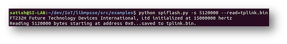
8. RETRIEVING THE FIRMWARE USING SPIFLASH:
We will use the spiflash.py script provided in the examples of libmpsse to dump data from the GD 25Q32C SPI Flash Memory.
Use the following command to dump data from the SPI Flash Memory:
python spiflash.py -s <<no of bytes to dump>> --read=tplink.bin
We will try to dump a random amount of data, for example 5120000 bytes.
Command: python spiflash.py -s 5120000 --read=tplink.bin
9. Exploring the firmware:
Let’s explore the tplink.bin file we dumped from the GD 25Q32C SPI Flash Memory using Binwalk.
Run binwalk tplink.bin to collect information of the binary.
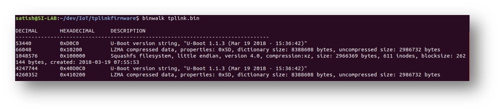
From the output we can observe that the dumped data contains a Squashfs filesystem, Universal Boot Loader (U-Boot). Once we extract the data we dumped, we can explore the Squashfs filesystem and U-Boot.
10. Retrieving the Firmware:
The next step is to extract the firmware, using the following command:
Command: binwalk -e tplink.bin 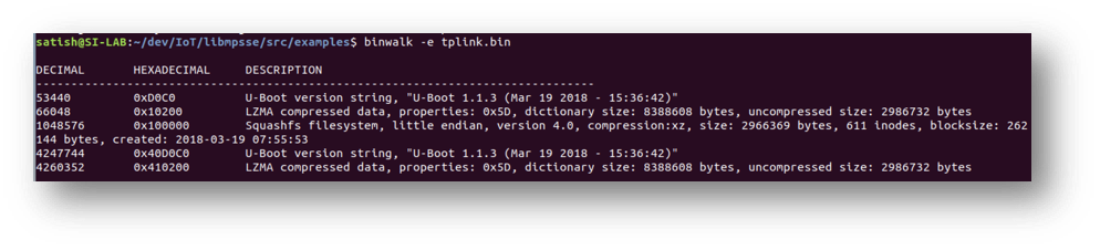
11. Exploring the extracted firmware:
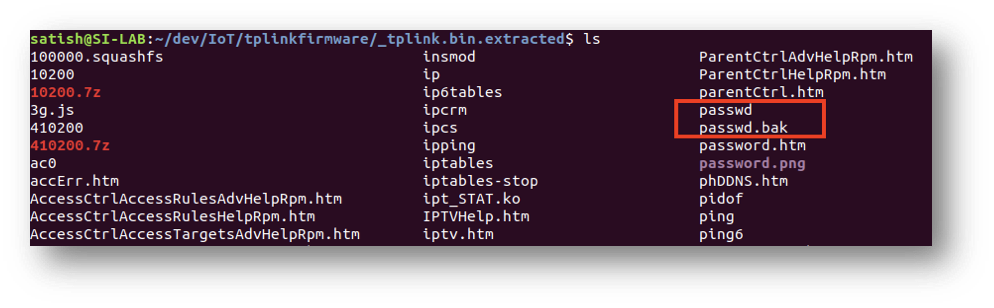
Observe the extracted directory _tplink.bin.extracted .
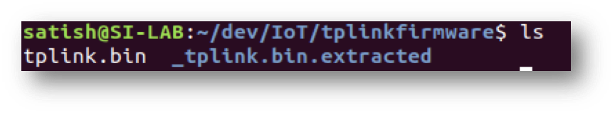
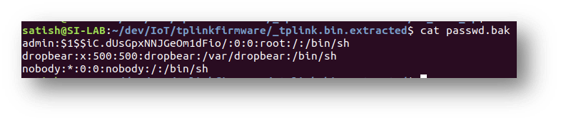
Let’s navigate to the extracted directory and explore the files. Observe that the passwd.bak file contains the password hash of the admin user.
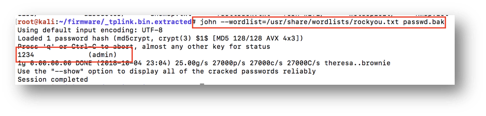
 5. 12. Cracking the password:
Now that we have access to the passwd.bak file, let’s try to get the plaintext password for the admin user. We will use John the Ripper and a popular wordlist (https://github.com/brannondorsey/naive-hashcat/releases/download/data/rockyou.txt ) to crack the hash.
john --wordlist=/usr/share/wordlists/rockyou.txt passwd.bak
John the Ripper has cracked the hash, and we get the plain text password as 1234 .
Conclusion
As illustrated, once we have access to the hardware, it is straightforward to dump data from a serial flash and gain access to stored secrets, code. From a pen testing perspective, exploiting hardware design issues and accessing secrets is sometimes much simpler than exploiting the supporting web interface or the mobile application.